Comprehensive DFT Solutions
Sanketh Semiconductors provides complete Design for Testability (DFT) services to ensure your ASIC/SoC meets production test requirements. Our DFT team has implemented test structures in 150+ designs across automotive, AI, and consumer applications, achieving >98% test coverage and reducing test costs by 30% for our clients.
We specialize in advanced DFT architectures for complex SoCs, including hierarchical test methodologies, at-speed testing, and low-power test solutions. Our DFT implementation supports nodes from 180nm to 5nm, with proven expertise in meeting zero-defect requirements for automotive (ISO 26262) and medical applications.
Our DFT Methodology
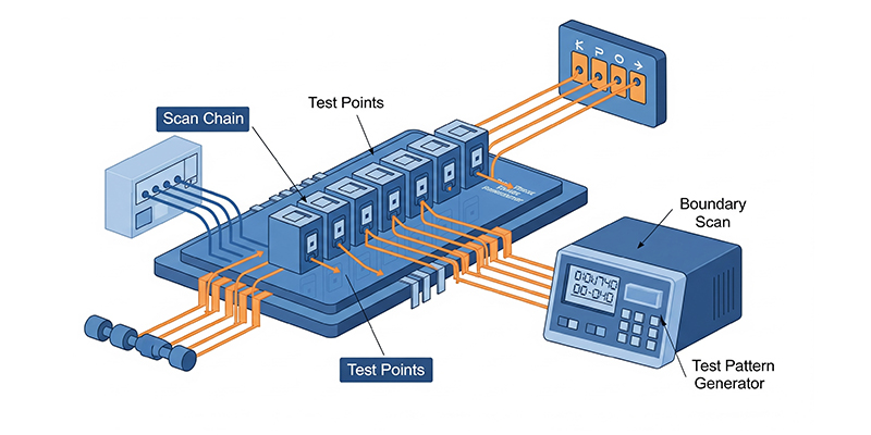
End-to-end testability solutions:
- Scan insertion (full/partial scan)
- ATPG and test pattern generation
- Memory BIST (MBIST) implementation
- Logic BIST (LBIST) integration
- Boundary Scan (JTAG IEEE 1149.1)
- Test compression (3-10X reduction)
Advanced DFT Capabilities
Our specialized DFT services include:
- Hierarchical DFT for large SoCs
- At-speed transition fault testing
- Power-aware test architecture
- Mixed-signal DFT solutions
- 3D IC test methodologies
DFT Infrastructure
We utilize industry-leading tools and flows:
- Synopsys DFT MAX, TetraMAX
- Cadence Modus, Jasper DFT
- Mentor Tessent platform
- Automated pattern validation
- Test cost analysis tools
Why Our DFT Services?
- 98%+ stuck-at and transition coverage
- 30% reduction in test pattern volume
- Zero-defect automotive solutions
- Seamless ATE handoff
- Production test support
Our DFT team works closely with your design and test engineering groups to develop optimal test strategies. We've helped clients achieve 40% faster test development cycles and 25% lower production test costs through our innovative DFT methodologies.